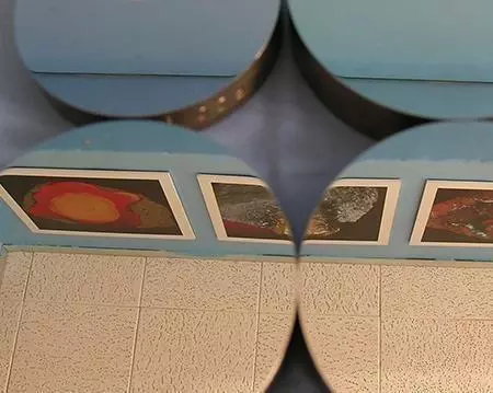
Surface Finishing for Optical Components and Photonics: Polishing Precision Optics
What is Precision Optics
Precision Optics is the science of using optical components and elements in electro-optic devices. It is an essential technology for the detection, transmission, sense, and effects of light energy. The technology works with light energy of specific wavelengths and the changes in its spectrum. The optical properties of materials are dependent not only on their geometry but also on the type of material used. Precision optics is useful for applications that require light for precise measurement, structuring, analysis, and processing with a higher level of accuracy. The achievement of a specific set of properties through the use of both glass and plastic optics is what is referred to as precision optics. The technology has introduced a whole new concept of very small lead times and delivery times as well. Modern concepts in precision optics have enabled the achievement of fast signal processing for light. Miniature devices and machines are continuously developed using precision optics materials. Precision optics finds application in various fields, such as laser optics, infrared optics, achromatic optics, and optical prisms. Laser optics is an essential technology that is used in many applications such as welding, cutting, and drilling. Infrared optics is used for night vision and thermal imaging applications. Achromatic optics is used to correct color aberrations, while optical prisms are used for reflection, refraction, and dispersion of light.
Photonics Engineering Technology
Photonics engineering is a field of engineering that focuses on the study of light energy and information to develop advanced technologies across various fields. It is an interdisciplinary area that integrates principles from physics, electrical engineering, and materials science to create innovative optical technologies. Photonics engineering is an essential technology for creating instruments for healthcare, construction, information technology, communication, and other industries. Photonics engineers are in high demand across a wide range of industries as they are needed to drive progress in this field. Efficient photonics devices are required to replace traditional light transmittance methods, and these can be developed using specialized engineering expertise. The field of photonics engineering has played a crucial role in advancing the communication industry by enabling higher efficiency and faster delivery times. The technology makes you capable of generating and studying nanostructured materials that can exceptionally perform well and be used in optical devices of the modern era. Photonics engineering identifies the techniques, tests, and procedures with which optical structures are visualized, monitored, amended, and used. Several elements are currently being created to enhance the effectiveness of electrical circuits in optoelectronic devices.
Applications of Photonics Engineering
Photonics engineering has numerous applications in various fields. It has helped in the development of new instruments for healthcare, such as medical imaging and diagnostics. The technology has revolutionized the telecommunication industry by introducing fiber optics for high-speed data transmission. It has also improved the manufacturing industry by enabling high-precision manufacturing. Photonics engineering has also contributed to the development of new materials, such as semiconductors, which are used in optoelectronic devices. These devices include solar panels, LED lights, and sensors. Photonics engineering has also played a vital role in the development of new information technologies, such as quantum computing.
Optoelectronics and Photonics: Understanding the Differences and Interconnections
Optoelectronics and photonics have distinct differences. Optoelectronics focuses on light emitting and detecting devices, whereas photonics is concerned with the physical science of light and its applications. Optoelectronics is a specialized electronics branch that specifically deals with optical applications, while photonics is mainly concerned with optics and the study of physical properties and phenomena. Optoelectronics explores the source of light, detection, and control, particularly for electronic devices' optical components like diodes and transistors. On the other hand, photonics is primarily focused on studying the physics of light and how it relates to optical phenomena. Optoelectronics leans towards the electrical implementation of a phenomenon studied in photonics. Both branches work together to develop optical devices for various applications ranging from household uses to space technologies.

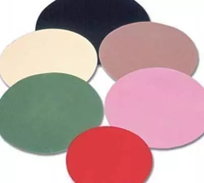
Surface Finishing Optical Components
The surface finishing techniques used in optical component manufacturing are dependent on the type of material and the required optical specifications. The technique of rotating or scanning optical components in a liquid is a frequently employed method for surface finishing. The following surface finishing techniques are used in optical component manufacturing:Polishing pads are used to achieve a smooth surface finish on optical components. To achieve a surface roughness level of up to 0.3 nm RMS value, ultra-polishing pads are utilized. Contact polishing and quasi-polishing pads are also used to achieve the required surface finish. Slurry jet polishing is a surface finishing technique used to achieve an improved surface finish on optical components. In this technique, a high-velocity slurry jet is used to polish the optical component.
Cleaning optoelectronic components is a crucial step in the manufacturing process. It involves removing dirt, dust, and other contaminants that may affect the optical properties of the material. The material must be cleaned efficiently to obtain optimal visuals and image creation.
Kemet provides exceptional surface finishing procedures for a wide range of optical components and materials. They provide high precision and accuracy in their processes, achieving optimal surface quality for the desired outcome. Their processes include precision lapping, polishing, and diamond machining. They also offer advanced cleaning processes for optoelectronic components.
Beta Barium Borate
Beryllium Copper
Surface Finishing Beryllium Copper - Material Test
The objective of the process was to achieve an optical finish without any specific flatness requirements. Various Beryllium Copper samples were used for the process.
The process involved three stages, each with specific plate/cloth type, abrasive type/grade, dispenser settings, and process time. The process breakdown is summarized in the table below:
Stage 1
The first stage involved using a Kemet 15” diamond lapping/polishing machine with a Kemet XP lapping plate and 3µ Type K STD diamond slurry. The component was subjected to a weight of 4 kg for 15 minutes to produce a good reflective finish. Some scratches were visible on the surface after this stage.
Stage 2
In the second stage, the component was run on an ASFL-AW silk cloth using 3µ Type K STD diamond slurry for 5 minutes with a weight of 4 kg. This pre-polishing stage prepared the component for final polishing and resulted in a 90% blemish-free finish.
Stage 3
The final stage involved polishing the component to achieve a blemish-free mirror finish. The component was run on a KemCol 15 - Chemical Mechanical Polishing Machine with a CHEM cloth and COL-K colloidal silica for 5 minutes with a weight of 4 kg.
The lapping and polishing process described in this case study resulted in a blemish-free mirror finish on Beryllium Copper samples. The process involved three stages using specific machines, plates, cloths, and abrasive slurries. The recommended equipment for running one component includes a diamond lapping machine, a colloidal silicate lapping machine, and other necessary accessories.
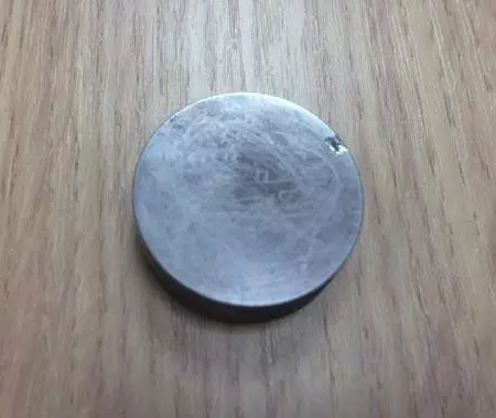
Before Polishing Beryllium Copper
After Polishing Beryllium Copper
Cadmium Sulfide
Calcium Fluoride
Fused Silica
Fused silica is the amorphous form of silicon dioxide used extensively in optical instruments such as lenses, mirrors, metrology components, and parts of optoelectronic devices. Surface finish is crucial for obtaining optimal reflective, refractive, and transmittance properties. To achieve this, abrasive powders such as cerium oxide particles are commonly used. Kemet has developed an effective polishing procedure that yields a highly flat and pure fused silica surface.
Gallium Arsenide
Germanium
Surface Finishing Germanium Parts - Material Test
The process to achieve the desired surface finish on the germanium discs involved two stages of lapping and polishing, using specific machines, lap plates, abrasives, and additional pressure.
Stage 1: In the first stage, a Kemet 15” diamond lapping/polishing machine was used, along with a cast iron lap plate and Kemox 0800S abrasive type/grade. An additional pressure of 4 kg was applied during the process. The germanium discs were lapped for 2 minutes per side.
Stage 2: In the second stage, the same Kemet 15” diamond lapping/polishing machine was used, but this time with an ASFL polishing cloth lap plate and Kemet Liquid diamond Type K 1 Micron standard abrasive type/grade. An additional pressure of 4 kg was again applied. The germanium discs were polished for 5 minutes per side.
The process used to lap and polish the germanium discs was successful in achieving the required surface finish. The flatness achieved was better than the required specification, and while the Ra achieved was slightly higher than the required specification, it was still within an acceptable range. The Rz achieved was well within the required specification. The use of specific machines, lap plates, abrasives, and additional pressure, along with careful monitoring and control of the process, enabled the desired surface finish to be achieved.
The required and achieved results for the germanium discs are as follows:
Flatness required: < 3 µm . Preferably 1 µm
Flatness achieved: 2 light band = 0.67 µm
Ra required Ra: 0.01 µm
Ra achieved: 0.059 µm
Rz required: 0.05 µm
Rz achieved: 0.0253 µm
Before Lapping & Polishing Germanium
After Lapping & Polishing Germanium

Lithium Niobate
Lithium Triborate
Magnesium Fluoride
Quartz
Surface Finishing Quartz - Material Test
Test Requirements: The test objective was to lap and polish two samples of quartz, a quartz glass tube with an outer diameter of approximately 62mm, and a quartz glass rod with an outer diameter of approximately 41mm. The target was to achieve flatness better than 1 µm and Ra better than 1 nm.
The process was divided into two stages, lapping and polishing, with the following details:
Stage 1 - Lapping: During the lapping stage, the cast iron plate was used along with Kemox 0-800s abrasive type and grade for a process time of 20 minutes. The glass was held on the weights using a non-slip film to prevent slipping during the lapping process.
Stage 2 - Polishing: After lapping, the PSU-M polishing pad was used along with Kemox WC abrasive type and grade for a process time of 50 minutes. The same weights and non-slip film were used to hold the glass in place during polishing.
Micracut 201 Precision Saw: The quartz sections were initially cut using a Micracut 201 precision saw with a diamond cutoff wheel and a slow feed rate. This process produced a clean cut with minimal chipping.
Results: After the lapping and polishing process, the middle of the parts achieved flatness of 1-2 light bands, which is less than 1 micron. Additionally, the Ra value was better than 1nm.
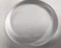
Before Polishing Quartz

After Polishing Quartz
PR3 Plate Quartz Polishing Test
Another test was conducted to evaluate the surface finishing process's effectiveness using a PR3 plate. The test involved a quartz workpiece of size φ100mm × 6mmT, and the in-situ method was used for polishing. The plate used was a 15” PR3 plate conditioned by facing the unit, and the rpm was set to 40rpm. Cerium oxide slurry of size 1~2 µm with 5% weight was used, with a flow rate of 5ml/min. The process was divided into two steps:
Process 1: Pressure of 80g/cm2 was applied for 30 minutes.
Process 2: Pressure of 30g/cm2 was applied for 20 minutes.
Results: The flatness result achieved was 0.130µm (λ/4.88).
Conclusion: Achieving the required surface finish on quartz components can be challenging, but it can be achieved using a combination of diamond lapping and polishing processes. The process can provide the required flatness and Ra values, making it suitable for various industrial applications.
Sapphire
Silicon
Silicon Carbide (SiC)
Surface Finishing Silicon Carbide - Material Test
Test Requirements: The objective of this test was to achieve the best surface finish on 65mmø silicon carbide blanks before pitch polishing. The material used was silicon carbide blanks.
Procedure: The surface finishing process was divided into three stages, each using a different machine, lap plate, abrasive type/grade, and additional pressure.
Stage 1: The first stage involved the use of a Kemet 15 diamond lapping/polishing machine with a Kemet iron lap plate with spiral grooves. The abrasive used was Kemet liquid diamond type K 14 micron standard, and the additional pressure was 3.5 kgs for one part. The dispenser setting was 2-second spray every 40 seconds, and the process time was 5-10 minutes for the front surface.
Stage 2: The second stage involved the use of a Kemet 15 diamond lapping machine with facing unit and a Kemet copper lap plate with spiral grooves. The abrasive used was 6-KDS1488 (water-based) diamond slurries, and the additional pressure was 4 kgs. The dispenser setting was 2-second spray every 40 seconds, and the process time was 10-15 minutes.
Stage 3: The third stage involved the use of a Kemet 15 diamond lapping machine with facing unit and a pure tin lap plate. The abrasive used was 0.75-KDS1438 (water-based) diamond slurries, and the additional pressure was 4 kgs. The dispenser setting was 2-second spray every 40 seconds, and the process time was 1.5-2 hours.
Results:
Stage 1: The first stage resulted in the removal of 10-20 µm of material in 5-10 minutes. The surface finish achieved ranged from 0.08~0.084µm.
Stage 2: The second stage provided a semi-reflective surface with a surface finish of Ra 0.056~0.060µm.
Stage 3: The third stage resulted in a mirror surface finish of Ra 0.007µm.
Based on the experimental results, it can be concluded that to achieve the desired surface finish and flatness, pitch polishing should be used. The flatness was measured on a Zygo and was 0.341 µm (Peak to Valley) after the final polishing of silicon carbide. These results show that the implemented surface finishing process was successful in achieving the desired surface finish and flatness for silicon carbide blanks.
After Stage 1 Polishing Silicon Carbide
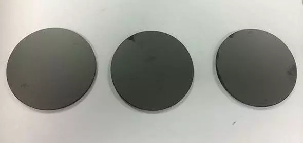
Final Flatness After Polishing Silicon Carbide
Yttrium Aluminum Garnet (YAG)
Zinc Selenide
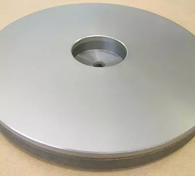
PR3 Polishing Plate For Optics
The Kemet PR3 Polishing Plate is a thermally stable resin plate that provides an alternative to polyurethane pads for polishing precision optics. The plate can be used with cerium oxide, aluminum oxide, and diamond slurries. The Kemet PR3 can be supplied as complete plates in most diameters or as discs for fixing to your machine base plate.
Advantages of Kemet PR3 Polishing Plate
One of the significant advantages of using the Kemet PR3 Polishing Plate is its ability to produce excellent flatness. The plate has been designed to achieve flatness below 0.08 microns, which is ideal for polishing precision optics.
The Kemet PR3 Polishing Plate offers improved edge exclusion, which means that there is no fall off at the edges. This feature is essential for maintaining consistency in the surface finish of the polished optics. It is capable of producing excellent surface finishes down to 1 nanometer. This feature is critical for achieving the desired quality in the final product. It is easy to machine, making it an ideal choice for polishing optical glass. The plate can be easily shaped and configured to meet the specific requirements of the optical component being polished. It is an excellent alternative to using polyurethane pads for polishing precision optics. The plate offers several advantages, including excellent flatness, improved edge exclusion, the ability to produce excellent surface finishes, and easy machineability. These features make the Kemet PR3 Polishing Plate an ideal choice for polishing optical glass and other precision optics.