Advanced Surface Finishing for Photonics, LED and Precision Optics: Polishing for Enhanced Optical Performance
Optical components play a significant role in modern technology, including telecommunication, medical imaging, scientific research, and manufacturing processes. To achieve optimal optical performance, optical components require high-quality surface finishing. Surface finishing is a critical step in the manufacturing of optical components. The appropriate surface finishing technique must be selected based on the type of material and the required optical specifications. Kemet provides exceptional surface finishing solutions for a wide range of optical components and materials, ensuring high precision and accuracy in their processes.
The surface finishing techniques used in optical component manufacturing are dependant on the type of material and the required optical specifications. The technique of rotating or scanning optical components in a liquid is a frequently employed method for surface finishing. The following surface finishing techniques are used in optical component manufacturing:
Polishing pads are used to achieve a smooth surface finish on optical components. To achieve a surface roughness level of up to 0.3 nm RMS value, ultra-polishing pads are utilised. Contact polishing and quasi-polishing pads are also used to achieve the required surface finish. In contact polishing, the optical component is pressed against the polishing pad to achieve a uniform surface finish. Quasi-polishing is a similar process, but it uses a specially designed polishing pad to achieve the desired surface finish.
Slurry jet polishing is a surface finishing technique used to achieve an improved surface finish on optical components. In this technique, a high-velocity slurry jet is used to polish the optical component. The slurry jet contains abrasive particles that impact the optical component at high velocity, resulting in a smooth surface finish.
Precision lapping is a process used to produce flat and parallel surfaces on optical components. In this process, a series of abrasive particles are used to remove material from the optical component. The process is repeated until the desired flatness and parallelism are achieved. Diamond machining is a process used to achieve high precision and accuracy in the surface finishing of optical components. Diamond tools are used to remove material from the optical component, resulting in a smooth surface finish. The process is particularly useful for hard and brittle materials such as sapphire, quartz, and ceramics.
Cleaning optoelectronic components is a crucial step in the manufacturing process. It involves removing dirt, dust, and other contaminants that may affect the optical properties of the material. The material must be cleaned efficiently to obtain optimal visuals and image creation.
Kemet provides exceptional surface finishing procedures for a wide range of optical components and materials. They provide high precision and accuracy in their processes, achieving optimal surface quality for the desired outcome. Their processes include precision lapping, polishing, and diamond machining. They also offer advanced cleaning processes for optoelectronic components.

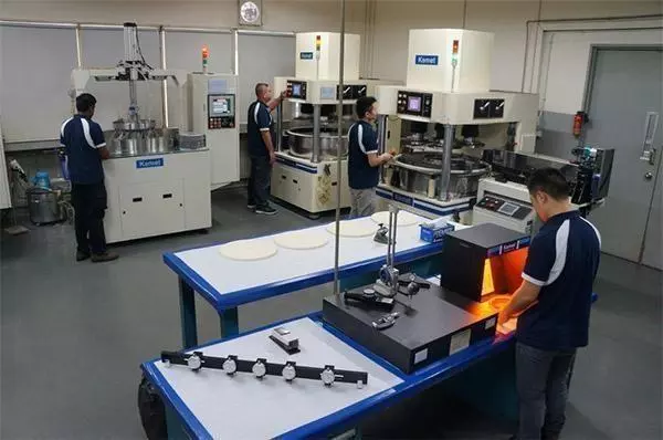
Lapping and polishing are critical processes in the LED industry for achieving the desired level of precision and quality in the production of various LED components. Kemet is a leading provider of lapping and polishing products designed specifically for use in the LED industry.
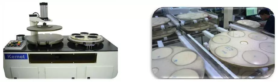
Kemet Dual Face Grinding, Lapping & Polishing Machines feature a 4-way motion and variable speed drive, which can execute complex routines while producing precise and repeatable results on a wide variety of materials. These machines come with options to build with HMI control, Automatic Thickness Control, and Load Cell for precise pneumatic pressure and parts dimensional controls during lapping and polishing operations. They are highly versatile and can be used for a range of applications, including: Sapphire Wafers, Silicon Wafers, Precision Optics, Filter Glass, Sapphire Watch Glass, Quartz Crystals Disk Drive Components
Kemet XJ Machines are heavy-duty single-sided precision lappers and CMP polishers applicable to a wide variety of processes for mass production. These machines are highly efficient and are used for a variety of applications, including: LED substrates, Silicon wafers, Magnetic heads, Hard disk drive components, Facing and Grooving Units
Kemet Facing and Grooving Units are used for the efficient lapping and polishing of flat surfaces, and for cutting or grooving circular parts. These units can be customised to meet the specific needs of different LED applications. Kemet Wax Bonders are used for bonding wafers, substrates, and other components with precision and accuracy. They are an essential tool for the LED industry and can help achieve the desired level of quality and precision in the bonding process.
Zygo Measurement: Surface Roughness and Tropel Measurement: Total Thickness Variation are two of the most important aspects of the lapping and polishing process in the LED industry. Kemet provides these measurement services to its customers, ensuring that their products meet the required quality standards.
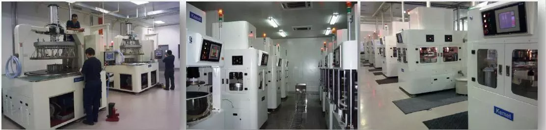
Kemet offers training and technical support services to its customers. These services are provided in Kemet's fully equipped workshop and cover a range of topics related to lapping and polishing technology, including process development, troubleshooting, and maintenance. Kemet's Far East presence in Singapore and the Asia Pacific region allows the company to serve the latest manufacturing activities in research and development. Kemet regularly assists customers by developing new products and processes, utilising the latest precision flat lapping technology, and diamond abrasive technology. Customers' samples are evaluated free-of-charge, and comprehensive reports are issued covering all aspects of the processes, inspections, and the likely consumables cost involved.
Beta Barium Borate
Beryllium Copper
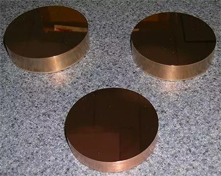
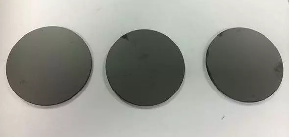
Surface Finish of Beryllium Copper using Lapping and Polishing
In this case study, we aimed to achieve a blemish-free mirror finish on various Beryllium Copper samples without specific flatness requirements. The lapping and polishing process involved three stages, each with specific equipment and parameters.
For the first stage, a Kemet 15” diamond lapping/polishing machine with a Kemet XP lapping plate and 3µ Type K STD diamond slurry was used. The component was subjected to a weight of 4 kg for 15 minutes, resulting in a good reflective finish, but with some visible scratches.
In the second stage, the component was pre-polished on an ASFL-AW silk cloth using 3µ Type K STD diamond slurry for 5 minutes with a weight of 4 kg. This step prepared the component for final polishing, resulting in a 90% blemish-free finish.
The final stage involved polishing the component to achieve a blemish-free mirror finish. The component was run on a KemCol 15 - Chemical Mechanical Polishing Machine with a CHEM cloth and COL-K colloidal silica for 5 minutes with a weight of 4 kg.
The recommended equipment for running one component includes a diamond lapping machine, a colloidal silicate lapping machine, and other necessary accessories. This three-stage process can result in a blemish-free mirror finish on Beryllium Copper samples, with each stage utilising specific machines, plates, cloths, and abrasive slurries.
Before Polishing Beryllium Copper
After Polishing Beryllium Copper
Cadmium Sulfide
Calcium Fluoride
Fused Silica
Fused silica is an amorphous form of silicon dioxide used extensively in optical instruments like lenses, mirrors, metrology components, and parts of optoelectronic devices. Obtaining optimal reflective, refractive, and transmittance properties requires excellent surface finish. To achieve this, abrasive powders like cerium oxide particles are commonly used. Kemet has developed an effective polishing procedure that yields a highly flat and pure fused silica surface.
Gallium Arsenide
Germanium
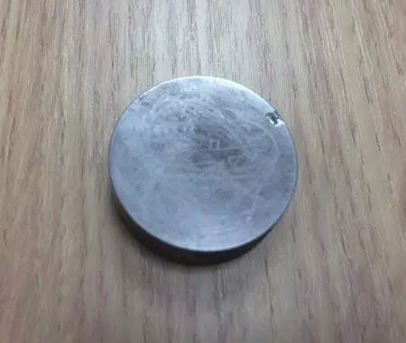
Surface Finishing Germanium Parts using Lapping and Polishing
Germanium parts surface finishing material test using lapping and polishing processes. The process involved two stages using specific machines, lap plates, abrasives, and additional pressure. The first stage used a Kemet 15" diamond lapping/polishing machine with a cast iron lap plate and Kemox 0800S abrasive type/grade. The second stage used the same machine with an ASFL polishing cloth lap plate and Kemet Liquid diamond Type K 1 Micron standard abrasive type/grade. The process successfully achieved the required surface finish and achieved better flatness and Rz than required. Although the Ra achieved was slightly higher than the required specification, it was still within an acceptable range.
Before Lapping & Polishing Germanium
After Lapping & Polishing Germanium

Lithium Niobate
Lithium Triborate
Magnesium Fluoride
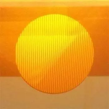
Quartz
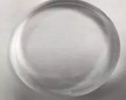
Surface Finishing Quartz using Lapping and Polishing
In this material test, two quartz samples, a glass tube with an outer diameter of approximately 62mm, and a glass rod with an outer diameter of approximately 41mm were lapped and polished to achieve a flatness of better than 1 µm and an Ra of better than 1 nm. The process involved two stages, lapping and polishing, with specific abrasive types and grades, along with the use of weights and non-slip film to hold the glass in place during the process. Prior to lapping and polishing, the quartz sections were precisely cut using a Micracut 201 precision saw with a diamond cutoff wheel and slow feed rate. After the process, the samples achieved a flatness of 1-2 light bands, less than 1 micron, and an Ra value better than 1 nm.
Before Polishing Quartz

After Polishing Quartz
PR3 Plate Quartz Polishing Test
A test was performed to assess the effectiveness of a surface finishing process on a quartz workpiece using a PR3 plate. The in-situ method was utilised for polishing, and a cerium oxide slurry of size 1~2 µm with 5% weight and a flow rate of 5ml/min was used. The process involved two steps: Process 1 with 80g/cm2 pressure for 30 minutes and Process 2 with 30g/cm2 pressure for 20 minutes. The achieved flatness result was 0.130µm (λ/4.88). Although achieving the desired surface finish on quartz components can be difficult, a combination of diamond lapping and polishing processes can deliver the required flatness and Ra values, making it suitable for various industrial applications.
Sapphire
Silicon
Silicon Carbide (SiC)
Surface Finish Silicon Carbide using Lapping and Polishing Techniques
Objective: The aim of this test was to achieve optimal surface finishing on 65mmø silicon carbide blanks before pitch polishing, using a three-stage process.
Test Requirements: Silicon carbide blanks were used, and the process involved different machines, lap plates, abrasive types/grades, and additional pressure at each stage.
Process:
Stage 1: Used a Kemet 15 diamond lapping/polishing machine with a Kemet iron lap plate with spiral grooves. The abrasive used was Kemet liquid diamond type K 14 micron standard, and the additional pressure was 3.5 kgs for one part. The dispenser setting was 2-second spray every 40 seconds, and the process time was 5-10 minutes for the front surface.
Stage 2: Used a Kemet 15 diamond lapping machine with facing unit and a Kemet copper lap plate with spiral grooves. The abrasive used was 6-KDS1488 (water-based) diamond slurries, and the additional pressure was 4 kgs. The dispenser setting was 2-second spray every 40 seconds, and the process time was 10-15 minutes.
Stage 3: Used a Kemet 15 diamond lapping machine with facing unit and a pure tin lap plate. The abrasive used was 0.75-KDS1438 (water-based) diamond slurries, and the additional pressure was 4 kgs. The dispenser setting was 2-second spray every 40 seconds, and the process time was 1.5-2 hours.
Results:
Stage 1: The first stage resulted in the removal of 10-20 µm of material in 5-10 minutes. The achieved surface finish ranged from 0.08~0.084µm.
Stage 2: The second stage provided a semi-reflective surface with a surface finish of Ra 0.056~0.060µm.
Stage 3: The third stage resulted in a mirror surface finish of Ra 0.007µm.
To achieve the desired surface finish and flatness, pitch polishing should be used. The flatness was measured on a Zygo and was 0.341 µm (Peak to Valley) after the final polishing of silicon carbide. The results show that the implemented surface finishing process was successful in achieving the desired surface finish and flatness for silicon carbide blanks.
After Stage 1 Polishing Silicon Carbide
Final Flatness After Polishing Silicon Carbide
Yttrium Aluminium Garnet (YAG)
Zinc Selenide
PR3 Polishing Plate For Optics
The Kemet PR3 Polishing Plate is a resin plate that is thermally stable and provides an alternative to polyurethane pads when polishing precision optics. The plate is compatible with diamond, cerium oxide, and aluminium oxide slurries and is available as complete plates or discs for easy installation. Using the Kemet PR3 Polishing Plate provides several advantages. Firstly, it has been designed to achieve flatness below 0.08 microns, ensuring excellent flatness during polishing. Additionally, it offers improved edge exclusion, maintaining consistency in surface finish across the entire polished area. The plate can produce surface finishes as low as 1 nanometre, which is essential in achieving high-quality results. It is also easy to machine and can be shaped to meet the specific requirements of the optical component being polished. The Kemet PR3 Polishing Plate is an excellent alternative to polyurethane pads for polishing precision optics, offering superior performance and quality.